The application I have in mind for my future Parallella board is to use it for various software-defined radio (SDR) applications. Given the small form factor, low power and high computing power of the Parallella, it would be ideal for a wide range of embedded uses. I can imagine portable battery powered units that are always ready to explore the spectrum around you, or even radio remote heads where you just place the radio and antenna in some remote location and only access it via network, with the bulk of the SDR work being done on the board itself and only sending back the data payload rather than raw radio samples.
To accomplish this, the first problem is to bridge the RF world with the digital one; some way to convert radio waves into digital samples and vice versa.
Of course, there are several solutions that could be plug-n-play, like rtl-sdr sticks, HackRF, BladeRF, UmTRX, Ettus USRPs and so on. But all of those are primarily meant for PCs and they use standard PC interfaces like USB or Ethernet. In all of those, some significant part of the hardware is actually there only to drive those standard interfaces! In the Parallella, there is a FPGA, and exposed are 48 high speed GPIOs that can be programmed to do … well … anything, and implement any kind of native IO protocol a radio front end might need.
This is where the MyriadRF comes in. This tiny board is sort of a demonstration board for the LMS6002D RFIC. It’s designed by Lime Microsystems themselves and it’s also fully Open Hardware. This particular chip is pretty great: it’s essentially a full duplex radio in a chip, capable of receiving and transmitting up to 28 MHz bandwidth signal anywhere from 300MHz up to 3.8GHz. And to top it off, the manufacturer has a very friendly attitude towards OSS and OSHW, with all documentation for the chip freely available (see here), a mailing list to discuss issues and they sent me a board so I could work on this application (Thanks Lime Micro 🙂 ). So it’s no surprise that a good number of new SDR hardware products based on it have popped up recently.
So, to come back to the topic at hand : how to use this MyriadRF ?
The board basically exposes the raw digital IQ interface of the LMS6002D chip, a SPI control port, a few GPIOs to control RF switches and some clock inputs. The clocks will have to be fed from some clock generator ICs (for various reasons, like phase noise, it’s not especially a good idea to try to feed these from an FPGA). But all the other ports could be plugged directly to FPGA IOs. When the time comes to actually design a daughter card, the GPIOs and SPI might be connected through I2C to leave more FPGA GPIOs free for other things. And with the final Parallella some level conversion will be required as well since the MyriadRF is 3v3 logic while the PEC_FPGA IOs are 2v5.
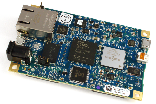
But all that is for later. I wanted something I could test NOW, with the Myriad RF I have and the Parallella prototype that is based on a ZedBoard. You can see below the setup I came up with. Basically I used the DE0-nano carrier board which is designed for the Myriad RF and it conveniently breaks out all the connections to the MyriadRF to standard .1 inch headers. It also includes a Silicon Labs clock generator IC. So far I have limited myself to the RX side and just wired all the data lines to some of the ZedBoard PMODs — the only thing to pay attention to is to connect the RX clock to a clock capable pin. As for the control lines, they’re currently driven by a Cypress FX2 on-board the DE0-nano carrier board, and controlled from the Parallella through USB. In future versions they’ll be driven directly from the FPGA, but as I said, for now I’m focusing on getting something running.

Test setup of the MyriadRF with the Parallella prototype
With the electrical connection done, the FPGA programming part could begin. Again in the spirit of getting something running quickly, I coded a simple interface to capture the samples and push them into a FIFO. The next step was to get them out of the FIFO and into the DDR with some block controlled from the ARM. For this part, I cheated a little and used a Xilinx tool called Vivado HLS which allowed me to write a quick-and-dirty AXI bus master in no time. The bad news is this tool isn’t available in the free WebPack edition of ISE, so I’ll probably rewrite that part in pure HDL to get more control and also allow a wide audience to rebuild the code.
Once all that was done, I could finally try to get some samples into the DDR and access them from the ARM. Currently there is no driver to speak of — just a couple of memory mapped control registers. And it doesn’t even allow a continuous gap-free stream, it just reads a few millions samples and places them into RAM. But this was enough to grab a couple of seconds worth of data and feed them to GNURadio to see the GSM carriers in the vicinity :

GNURadio showing captured samples of GSM activity
So what now ?
Well this is only the beginning. The HDL code has to be improved, a lot. A daughter-card has to be designed. A proper driver has to be written. A good way to ship all those samples to the Epiphany has to be found, possibly bypassing the ARM altogether. Much work left to be done 🙂