Last summer we started migrating the elink from Xilinx ISE to the new Vivado tools while also doing a complete overhaul of the design to improve performance, power, and maintainability. There is still optimization work to be done in terms of elink read/write performance, but I consider the new design to be a high quality starting point for future work. The new elink design project has been tested extensively at Adapteva and has recently gone through beta testing by friends in Sweden working on an exciting “non-parallella” Zynq + Epiphany board. More news on that development soon hopefully…
To anyone who has been stuck waiting for the new Vivado design, I am truly sorry for the delays! I am embarrassed that it has taken this long and I am doing everything I can to make sure this doesn’t happen again. A big part of this effort will be to more actively encourage contribution from outside Adapteva. Please consider this an open invitation to anyone with FPGA skills to contribute pull requests to the ‘parallella-hw’ repo. If you feel like there are barriers in the way, tell me how we can remove those. Together we can move faster.
The rest of this post is dedicated to getting you up and running with the elink and Vivado. For those of you who have never created HW before, this could be your first time:-)
STEP 1: Download and Install the Vivado software
You will need to follow the Xilinx instructions to download and install the Vivado 2014.3 suite. Start HERE.
Note#1: The download is large (>>1GB), be patient.
Note#2: Due to permission issues, it’s easiest to install it in it in your home directory.
Note#3: If you are running Ubuntu, edit the install script to use ‘/bin/bash’ instead of ‘/bin/sh’ (or change /bin/sh to point to bas instead of dash)
STEP 2: Download and unzip the Parallella project
$ wget https://raw.github.com/parallella/parallella-hw/master/fpga/vivado/releases/parallella_7020_headless.xpr.zip

$ unzip parallella_7020_headless.xpr.zip
Note: Currently as of March 22 a headless 7020 project is available. (parallella_7020_headless.xpr.zip)
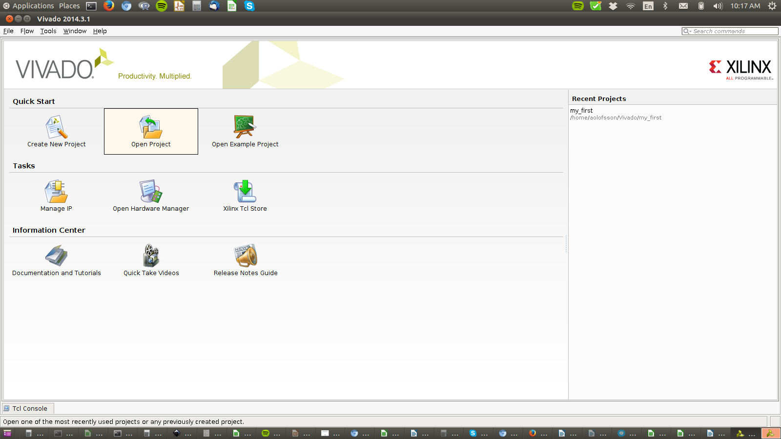
STEP 3: Open the archived Vivado Project
Click the ‘open project’ and point to the *.xpr file inside the folder you just unzipped.
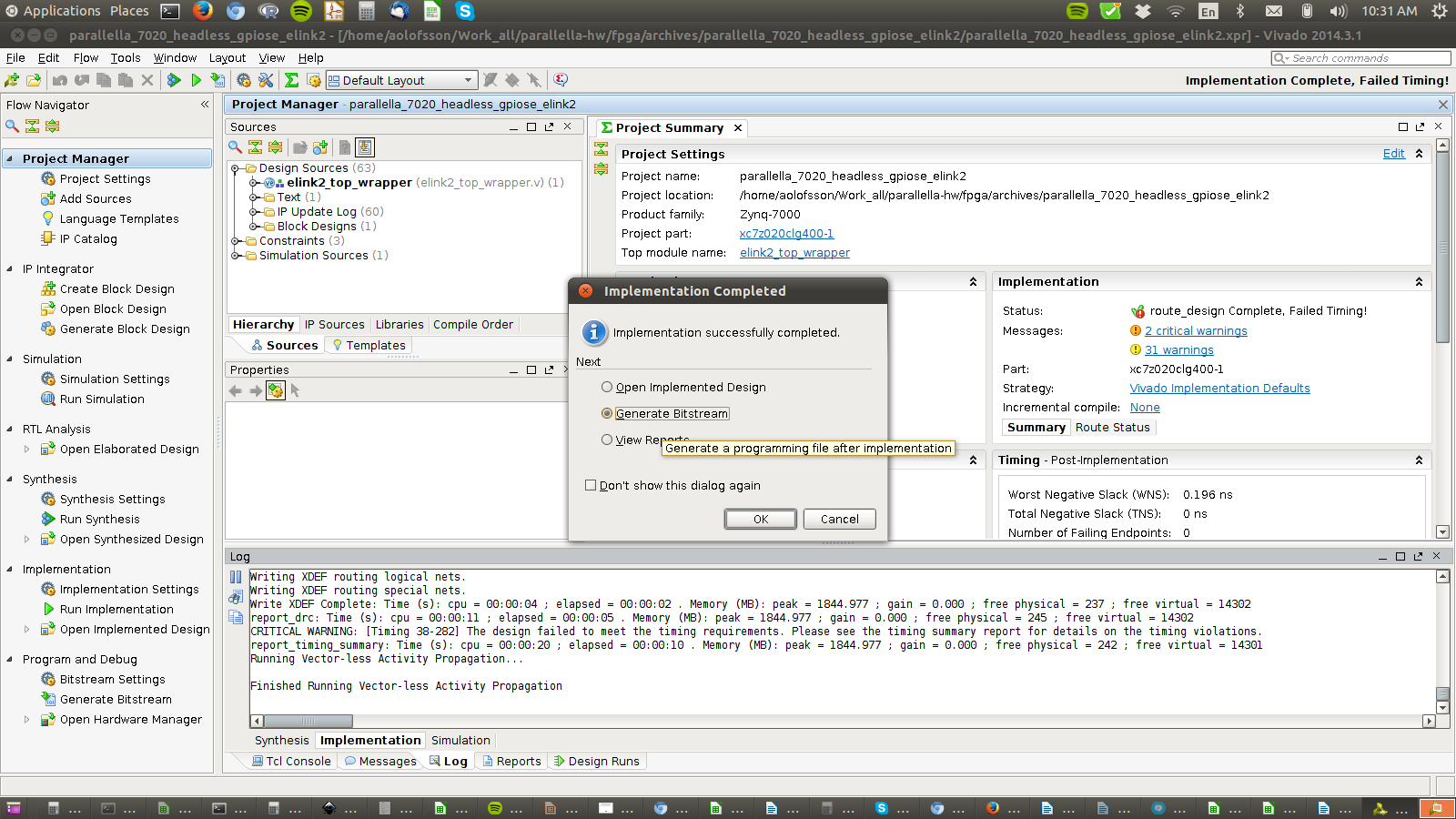
STEP 4: Run Synthesis
This step converts the Verilog RTL to a gate level netlist and optimizes the logic.
Find the right button to press in the GUI shown in the picture (or press F11).
(Ignore any warnings for now…)

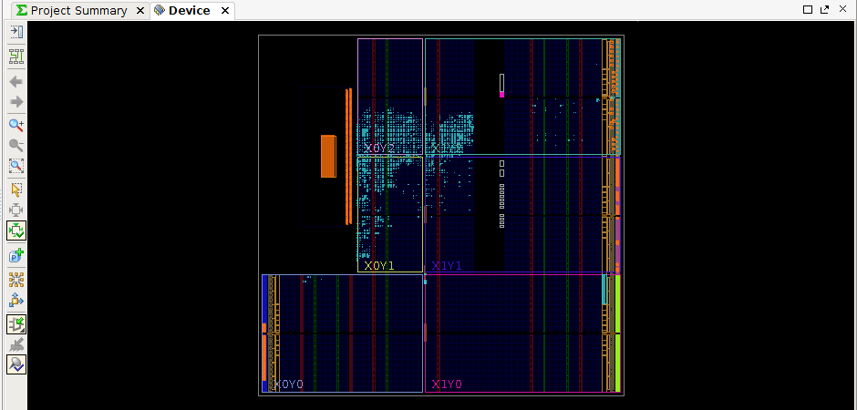
STEP 5: Run Place and Route
This step maps the gate level netlist to the physical hardware inside the Zynq FPGA.
(Ignore any warnings for now…)

STEP 5: Create the raw bitstream
(Ignore any warnings for now…)
STEP 6: Tweak the bitstream
There may be a better way of doing this…and if there isn’t there should be!! More than once I have forgotten to do this and gotten the error message: “Error: Timeout waiting for FPGA to config.
a. Create a file called ‘bit2bin.bif’ with the following content
 the_ROM_image:

{

[bootloader]dummy.elf

elink2_top_wrapper.bit

}
b. Make sure you have a dummy.elf in that directory. You can copy use this one.
c. Run some “magical steps” using the Xilinx tools to convert the bit stream to a loadable bit stream.
$ source $XILINX_INSTALL_PATH/Xilinx/Vivado/2014.3.1/settings64.sh

$ bootgen -image bit2bin.bif -split bin
STEP 7: Copy the new *.bit.bin file to the boot partion of a Parallella SD card.
Note: Sync and properly eject the sd card as appropriate for your system.
STEP 8: Boot the system.
Run some tests and report back if you have any issues.